Agilent Technology’s ADS handles “3D planar” topologies, which means that there are only a few discrete values for the z coordinate, and all edges are either horizontal or vertical. For this reason they can use the 2D Arrangement package for the representation of each different z level.
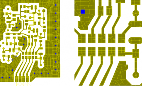
In the image you see a tri/quad mesh of a small RF board generated using CGAL Arrangements as backend representation.
The mesh is explicitly denser near the outer edges of the metallization because more accuracy is needed there.
The problem size is still very small with 11204 internal edges (meshing of a far more complex boards with about million internal edges is feasible).


